Production Test

Introduction to Structural IC Production Test
This document describes structural production test issues and techniques used to test digital IC.
License: Creative Commons Attribution 4.0 International.
See: creativecommons.org/licenses/by/4.0/
1.0 Table of Content

2.0 Structural Production Test Introduction 4
2.1 What is structural production test 4
2.3 Defects and their Sources 5
2.3.1 Physical Defect Sources 5
2.4.1 SSF - Single stuck-at-fault model 6
2.4.3 Delay fault model (Transition/Path Delay Faults) 6
3.1.1.1 Circuit with logic redundancy 8
3.1.1.2 Circuit with sequential redundancy 9
3.1.1.3 Tristate untestable circuit 9
3.1.1.4 Uncontrollable circuit 9
3.1.1.5 Unobservable circuit 9
3.1.2 Removing Untestable faults 9
3.2.7 Disable Active Preset 16
3.2.9 Make Latches Transparent 16
3.2.10 Clock feeding into combinatial logic 17
3.6.1 DFT Methodology questions 18
3.6.2 General design DFT issues 18
3.6.4 Physical design DFT issues 19
4.4.1 P1500 Mandatory Instructions 23
4.4.2 P1500 Optional Instruction 23
4.4.3 Core Test Language (CTL) - P1450.6 24
5.0 Automated Test Pattern Generation (ATPG) 24
5.1.1 Combinatial ATPG Rules (summary) 25
5.1.2 Combinatial Tester flow 26
5.2.1 Sequential ATPG Rules (summary) 27
5.2.2 Sequential Tester Flow 27
10.0 Built In Self Test (BIST) 29
11.0 Boundary Scan Test (IEEE 1149.1) 32
11.1.3 Instruction Register 35
2.0 Structural Production Test Introduction
This report covers some of production test techniques used to test digital ICs and tries to highlight various issues behind production test of today’s ICs. Production test does not intend to test functional correctness of an IC, even though it could be used to help to functionally verify it or debug it.
2.1 What is structural production test
Structural production test is a method of testing ICs geometrical structures rather than its intended function. It tries to establish if the produced IC is free of defects introduced by not always perfect manufacturing processes.
Chips can be tested by following methods:
- Functional test - is mainly used to test timing of a device under test (DUT) and clock transfers between different clock domains.
- Production test - scan, built in self test (BIST) and IDDQ test are testing structural functionality of the DUT.
- Boundary scan - is mainly used to test interconnections on PCB and bonding. However it is universal enough, so it can be also used for limited functional tests (usually not at full speed).
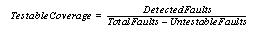
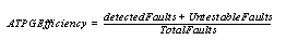
Quality of test is determined by its fault coverage. Fault coverage correlates to defect coverage and might be used as an indicator for establishing acceptable production yield.
Yield is the fraction of acceptable parts among all fabricated parts.
Tests are performed by a tester whether it is external or internal (BIST) to the IC. The tester does fault detection by applying input stimuli into DUT and observing their output response. If the DUT’s response is different than expected one, the DUT fails the test. The tester can then continue with the test in order to collect failure data or abort the test.
In order to be able to successfully test a DUT, it is in most cases necessary to insert special test structures (logic) into DUT. Process of inserting test structures into a netlist is called test synthesis (in this document).
Generation of input stimulus and corresponding response is called automated test pattern generation (ATPG).
2.2 Why to Test?
Testing ICs is an important way how to detect faulty devices which would otherwise be packaged and assembled on printed boards. The purpose of detecting faulty devices early in production is to reduce the cost of packaging and board repair. Therefore chips are tested before packaging, after packaging (this might be done by JTAG on the board) and sometimes even after board assembly.
An important part of every product production is to achieve a target production yield. In order to be able to achieve the target yield the manufacturer has to be able to monitor it. Production yield in IC production is a combination of IC foundry’s and packaging yield. Production test is giving the manufacturer a means of sorting the bad devices from the good ones, so they can trash them and they can estimate what the yield is. Statistically analyzing detected faults, their location and relationship to the manufacturing process (bit / logic mapping) can help to improve the process and increase the yield. As no present production test technique are perfect, there are test escapes. Due to their high cost, it is necessary to keep test escapes as low as possible. The next chapters might give you an idea how it could be done.
2.3 Defects and their Sources
Faulty ICs are caused by defects and errors in their manufacturing process. In order to be able to detect these manufacturing defects without altering the ICs characteristics, the testing has to be done through electrical observation of the circuit properties. To be able to do that, a electrical models has to exists for the production defects.
2.3.1 Physical Defect Sources
Defects in an IC are typically caused by one or a combination of the following factors.
2.3.2 Electrical Defects
Electrical defects are electrically quantized results of the physical defects.
2.3.3 Logical Defects
Logical effects are logical abstraction of actual device defects.
Faults are result of physical defects. Direct not destructive detection of physical faults would be very difficult (expensive), slow and in some cases impossible. Additionally physical defects do not allow a direct mathematical treatment of testing and diagnostics. Therefore logical models of faults are used for test. Logical faults represent the effect of physical faults on the behavioral of the modeled system. Faults can affect logic function (fuctional faults) or/and timing (delay faults) of a system.
The effects of the physical defects on their Electrical and / or Logical models are dependent on technology’s geometrical properties. With ever shrinking feature size, gate oxide thickness, lower voltage and changing geometry proportions of wiring of today’s deep sub micron (DSM) ICs, the effect of a physical defects have more significant impact on the ICs correct function. For example:
- Wiring geometrical properties are very different in DSM technologies than in technologies with feature size > 0.18 um. In technologies bellow 0.18 um and especially with Cu interconnects wire delay variations, accidental wire cross talk, reliability of metal layers vias, probability of bridging faults, etc. have much higher statistical probability than in older technologies with bigger feature size.
- Thinner gate oxide is more sensitive to contamination and lithography defects than thicker gate oxide of older technologies.
- Higher leakage current in DSM technologies makes IDDQ testing more difficult and less effective.
All the issues listed above as well as other DSM issues not mentioned here can significantly affect the reliability of electrical characteristics of the circuit and currently available fault models. One can expect new fault models emerging in the future. That will lead to new tests being added to production test sets and greater complexity and perhaps higher cost of chip production test in the future
2.4 Fault Models
Fault models are used to model various physical defect mechanisms mentioned in chapter Defects and their Sources. The physical defects therefore can be measured as either electrical or logical quantification of the defects. This chapter mentions the four most used fault models in the industry today.
The fault models mentioned below are valid under the single fault assumption, where a test guarantees the detection of a fault only when no other fault is present.
A fault is a logic level abstraction of a physical defect that is used to describe the change in the logic function of a device caused by the defect.
2.4.3 Delay fault model (Transition/Path Delay Faults)
- used to detects path delays longer than time required for safe capture
- difficult to apply test patterns (launch on capture) or high area overhead (launch on shift) for mux scan test methodology
- lower fault coverage (unless LSSD)
Transition delay faults - model the time between an input change and corresponding output response of a gate. It is more sensitive to local random process variations.
Path delay faults - model the cumulative gate + wire line delays along a timing path. It is good at detecting both local random process variations as well as global process (propagation) shifts.
Delay fault models can detect physical defects like: low transistor channel conductance, narrow interconnect lines, treshold voltage shifts, resistive vias, IR drop, some opens and even cross talk (cross talk is not a manufacturing, but design fault).
Practical studies suggest that random patterns can be just as effective in detecting delay faults as ATPG generated deterministic patterns.
Delay faults require two test patterns - one to initiate the circuit and the second one to propagate the change. This is due to the fact, that delay fault detection is in fact a transition detection.
Circuit for delay fault testing should not have any multi cycle and false paths as they would be untestable and could invalidate the single fault assumption of the DUT.
2.4.5 Burn In Test
Burn-in test is a temperature stress test. Burn in is important as some chips, that pass production test will fail shortly after the test. It is possible to say that burn-in forces failures in weak/soft devices through temperature accelerated aging.
Burn-in test activates so called infant mortality failures caused by process variation in variation sensitive design and also so called freak failures caused by the same mechanism as failures in good devices. The most used of the two is the infant mortality detection as it requires short term burn-in (about 20 hours). The freak failure detection requires burn-in in order of 100s of hours and that makes it expensive.
3.0 Design For Test (DFT)
Design for test is set of design rules and design modifications used to improve testability of the DUT.
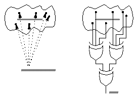
Without any circuit modification, any IC would have to be tested by a functional test, regardless whether the test pattern have been generated automatically by SW or by hand by an engineer. While this functional test could potentially determine correct function of an IC, in most cases it would not be able to verify correct function of each gate and interconnect (structure) in the IC. Writing high (structural) coverage functional test patterns would be very time consuming and would lead to very high test pattern count. The theoretical minimum number of functional test vectors is:

where i is number of inputs and k is number of internal storage elements. Example: 1 Mgate IC with 185 inputs, 12 kDff and 2 Mb of RAM would have 2.012.000 storage elements. Even if we exclude the RAM and surrounding logic from testing we still have 12.000 storage elements, which equals to:

If we are testing the device at 1 GHz for the duration of the universe existence our test would now be at combination about 3.2 x 1026 (3.156x10⁷ sec/year, universe is about 10 billion years old)
The solution to this problem is taking advantage of one or combination of the design for test (DFT) methodologies described in next chapters. There are two basic techniques to increase testability of DUT, non scan and scan DFT.
3.1 Non Scan DFT
Non scan DFT are general rules used to improve combinatial controllability and / or observability of the combinatial parts of DUT.
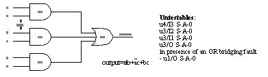
3.1.1 Untestable Faults
Untestable faults are faults which cannot be detected by any test. Since the presence of untestable (undetectable) faults do not have to change circuit functionality, it may appear that they are harmless and therefore can be ignored. However, a circuit with an undetectable fault may invalidate the single fault assumption.
From a test strategy point of view, it is assumed that one fault can be detected before the second one occurs. This may not be possible if the first one is undetectable. It could also mean, that complete test set (when all testable faults are covered by the test) may not be sufficient to detects all faults because of untestable fault.
3.1.2 Removing Untestable faults
3.1.3 Observe Trees
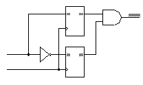
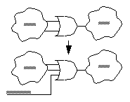
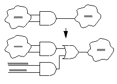
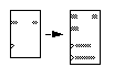
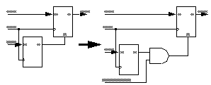
Observe trees technique is used to increase combinatorial observability of tested circuit. Difficult to observe points are connected to inputs of a XOR tree.There are no additional gates placed in the data path, so the timing impact of this technique is minimal. Output of the observe tree can be connected to a primary output or in case of scan DFT to additional (scan only) Dff.
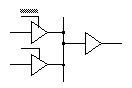
3.1.4 Cell Translation
Cell translation is used to improve controllability of the circuit. Targeted cells are replaced with functionally equivalent cell with one additional input connected to a special test pin. Timing impact of this method is low and depends on difference in delays of the original cell and its replacement.
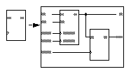
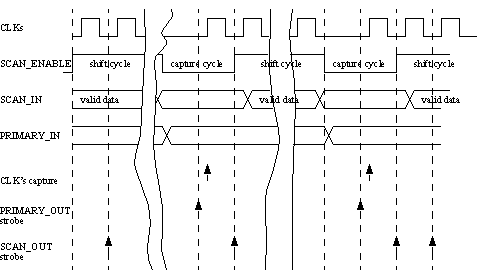
3.2 Scan DFT
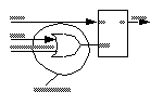
Scan test is a technique used for synchronous designs. Overall testability of a design is increased by replacing all or some of the storage elements (mainly flip flop gates) with their scan equivalents. All those replaced scan cells are then connected together to form a shift register called scan chain. See Figure 7. This scan chain adds additional control and observe points to the circuit and thus reduces sequential and combinatial complexity of the design. Functionality of the circuit with scan inserted is unchanged.
As a result of scan insertion, we can look at the design as a collection of combinatial blocks tested via their respective I/Os (this could be either ICs primary inputs (PI) and outputs (PO) or virtual PIs and POs - scan Dffs). For this reason both scan as well as non scan DFT rules apply.
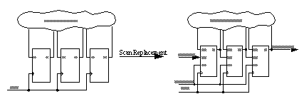
 FIGURE 7. Scan: Principal diagram
There are three type of scan methodologies supported in ASIC libraries:
3.2.1 Muxscan
- Advantages - Low area overhead
-
Disadvantages - Timing impact on design
Not suitable for delay/transition path delay faults
2 - additional pins (SI and SE)
Widely supported in ASIC libraries
3.2.2 LSSD
- Advantages - No timing impact on design
- Disadvantages - Almost double the area of LSSD cell over simple DFF
Best for latch based designs
Suitable for transition/path delay timing models
3.2.3 Dual CLK Scan
- Advantages - No timing impact on design
- Disadvantages - Medium routing impact
Improves sequential ATPG performance
3.2.4 Multiple scan chains
Multiple scan chains are used to decrease the number of test vectors necessary to test the DUT. The number of tester cycles is reduced by performing more scan (shift) and/or capture cycles in parallel thus reducing the scan chain length. See Figure 11. Multiple scan chains should be balanced (to have same length) in order to further optimize test vector count.
Functional input and output ports can be shared with input and outputs of a scan chain. The principle is outlined in following principle diagram.
3.2.5 Multiple Clocks
Multiple clocks can be used to form scan chains.
Please note, that there are timing issues associated with having multiple clock sequential elements mixed in one scan chain. The timing problems are with both functional as well as scan timing. This is because separate clock domains typically have different clock tree insertion delay and skew, especially in the case of different clock domains size.There are two possible timing issues:
- long path - data will not be correctly captured / shifted to associated scan cell
- race condition - data will propagate through more than 1 seq. cell
Matching clock insertion delay and skew is an obvious solution, but it is very difficult to balance the clock trees (especially the ones of different sizes) together in all operating conditions.
If there are multiple clocks in the design, there are following ways to deal with them:
- Separate scan chains for each clock domain (can solve scan path timing problem)
- Separate clock pins for each clock domain (this allows to capture in one clock domain at a time and it can solve both scan and functional path problem at the cost of increased test time)
- Scan chain order (can solve scan path timing problem)
- Scan data path lockup cells (can solve scan path timing problem, if the clock insertion delay + clock skew is not greater than 1/2 clock period between the following scan cells)
From the previous list of possible solutions is possible to conclude, that the major obstacle in mixing clock domains and clock edges in the design is not the scan path but the inter clock functional paths.
Following chapters will look at each possible solution closer.
3.2.5.1 Scan Chain Order
Correct ordering of flip-flops in a scan chain can help to eliminate:
- Multiple shift within 1 CLK cycle
- Avoid hold violations due to clock skew
- Minimize routing impact of the scan path
There are three possible ways how to sort flip-flops in a scan chain:
It is also possible to combine the three rules.
An alternative solution to the problem with multiple clocks is to have separate scan chains for each clock domain.
3.2.5.2 Lock-up Cell
Lock-up cells are used to solve clock skew, caused by different insertion delays of different clock trees, in a scan chain during the shift cycle. It can also be used in cases where excessive clock skew within one clock domain exists. See Figure 12 for example.
3.2.6 Multiple Clock Edge
Multiple edges sequential elements can be used to form scan chains. It is important to note that mixing multiple edge sequential elements cannot be recommended in the design because it causes many timing related problems in the flow. When there are multiple edge seq. elements in the design and they cannot be changed, they can be dealt with as follows:
3.2.7 Disable Active Preset
Logic is inserted into netlist to disable active reset which could otherwise reset a flip-flop during scan cycle. This modification should be done before scan chain insertion.
3.2.8 Muxed Clocks
Logic is inserted into netlist to disable internally generated clock signals which would not otherwise allow a flip-flop to be used as a part of a scan chain. This clock signal is connected through an inserted MUX to a direct clock signal. This modification is done before scan chain insertion.
3.3 Full Scan
Full Scan is type of design where:
- All sequential elements are made scannable by replacing them with scan equivalents
- Logic is inserted to bypass gated clocks and presets. Clocks and preset signals are directly controllable from PI.
- Logic is inserted to make non scan latches transparent
- No clocks are input of combinatial logic
3.4 Almost Full Scan
This method is based on combination of both combinatial and sequential ATPG (explained in Automated Test Pattern Generation (ATPG)). Most sequential elements (80%-100%) are made scannable. Usage of sequential ATPG allows presence of non-scannable storage elements (memories, non-scan latches, bus keepers, negative edge flip-flops) in design. This allows testing timing critical areas (where scan synthesis cannot be done) and some combinatially untestable faults.
- Combinatial ATPG engine is used for 1st pass. That will make ATPG fast with good vector compaction.
- Sequential ATPG engine is used in 2nd pass. In that pass remaining undetected and combinatially untestable faults can be detected.
Potential disadvantage of this method could be two vector sets on the tester.
3.5 Partial Scan
Principle of this method is, that only certain parts of the design are selected for scan insertion. The parts of the design not tested by scan can be tested by sequential ATPG or by functional test.
The reason for partial scan could be severe area or timing constraints.
Problem of this method is typically lower test coverage, long ATPG run times and the need to hold values of non scan Dffs unchanged during scan test. This could be achieved by clock gating of the parts of the design not tested by scan.
3.6 DFT Issues
This chapter summarizes some DFT specific design issues facing a DFT engineer.
Following list raises some basic questions which should be answered prior to a DFT implementation and ideally also before the design implementation phase.
3.6.1 DFT Methodology questions
- Which scan methodology will be used Mux-scan or LSSD?
- What is required, full or partial scan? (preferably full scan or almost full scan)
- Which fault models should be used to achieve the target yield (stuck-at, bridging, delay path models)
- Should the test be done hierarchically (P1500/CTAG) or flat
- IEEE 1149.1 (JTAG)?
- IDDQ?
3.6.2 General design DFT issues
- Do flip flops have a scan equivalent?
- Do flip flops have controllable clocks and presets?
- Are there any scan destructive flip flops? How many?
- How many clock domains?
- Is the clock and reset distribution strategy simple and transparent?
- How many clock transfers? (potential races)
- How many scan chains? (need/afford)
- Are there any negative edge storage elements? (preferably none)
- Are there any latches in the design? Can they be controlled to be transparent?
- Is there any redundant logic in the design?
- Is the design strictly synchronous without combinatial feedback loops and without clock signals driving combinatial logic?
- How many spare test pins?
- Are bidirectional I/O enables controllable?
- Tristate buses? Can their output enables be controlled in order to avoid congestion?
- Are there any timing critical areas? Should they be excluded from scan?
- Test signal buffering and hold time on scan path can increase congestion.
- Are there any memories? (bypass? control WE? boundary scan? BIST?)
- Are there any IP blocks? Are they hard or soft macros? Are the hard macros scannable and are the test vectors and coverage information available?
- Are the analogue blocks (macros) IDDQ ready? (memories, PLLs, LVDS, analogue blocks)
3.6.3 Power DFT issues
- High activity factor caused by scan during the test.
- Increased power consumption in inserted DFT logic in functional mode.
- Power domain crossings due to the scan paths and scan enable distribution needs to be handled.
- No floating nodes in test mode allowed. This might increase number of bus keepers in the design. This is because there cannot be any floating nets in the IC at anytime during the test.
While it would be possible to reduce overall power consumption of an IC by reducing test’s activity factor, it would have negative effect on test speed. Reduction of activity factor could be done by “power aware” ATPG or by partitioning the DFT. DFT can be partitioned by means of separate scan chains with individual clock source for each chain or by structured test methodologies such as P1500 / CTAG.
3.6.4 Physical design DFT issues
- Placement of scan netlist should be done according to functional constraints (disregard scan initially)
- Routing impact of scan path (scan might have to be re-ordered to lower wiring congestion, especially in not square floor plan shapes)
- Scan enable tree constraint for delay fault model (for muxscan and launch on shift test technique)
4.0 Scan Design Flow
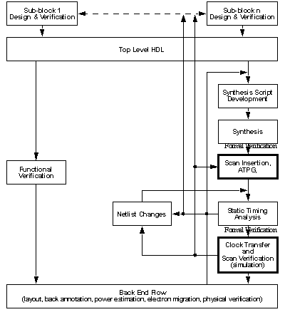
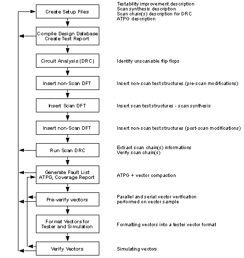
4.2 Hierarchical DFT Flow
Hierarchical test flow presented in this chapter is fundamentally similar to the top level test flow mentioned before. Hierarchical could be the DFT insertion, formal verification and test coverage analysis, test pattern verification as well as ATPG. However different combinations of hierarchical DFT insertion and top level ATPG flow are quite common. As the DFT is inserted and verified at the block level, great care must be given to the top level integration and planning in order to achieve good scan chain balancing and to avoid possible timing problems. As mentioned before ATPG can be done at top level (if the design size and ATPG tool capacity allows it). If ATPG is done at block level, top level test pattern expansion and block level test pattern assembly must be performed at the end of the flow. This step is similarly to the design top level integration.
This hierarchical approach increases capacity of the DFT flow (from the tool point of view), decreases overall tool runtime, reduces memory requirement, allow for early DFT problem detection and spreads the DFT tasks better trough the lifetime of the project.
If physical design (PD) hierarchy does not match the DFT hierarchy and ATPG is performed at block level, there might be problem with scan chain reordering in PD tools.
4.3 IP Test Packaging
IP blocks can be delivered as:
- scan ready - clean DFT DRC
- scan inserted - clean DFT DRC, inserted scan, resolved testability issues, target coverage achieved
- scan inserted + test patterns - does not need netlist, need for vector translation to the top
- BIST inserted - no need for netlist or test patterns, only bist control needs to be provided.
4.4 IEEE P1500
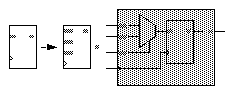
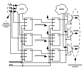
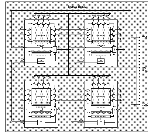
P1500 is designed for more structured and scalable approach to test of System On Chip (SOC) type of ICs. The idea of P1500 is based on an idea of an IC with multiple cores (can be IP) wrapped with boundary scan structures (similar to 1149.1). Those core wrappers provide the mechanism for both internal as well as external core test. The core test is done via user defined Test Access Mechanism (TAM). Whole test with its modes is controlled by Test Control Block (TCB).
Core Wrapper, Figure 18, provides following functionality:
- Functional - transparent wrapper cells
- Core test - application of stimuli to the core, capture test response, 3 state outputs can be set Z, core inputs can be forced to fixed values for safe state or IDDQ test, etc.
- Interconnect test - application of stimuli to the interconnects, interconnect values capture, 3 state outputs can be set Z, core output can be forced to fixed values
- Core isolation - core inputs can be forced to fixed (safe) values, core outputs can be forced to fixed (safe) values
- Optional parallel TAM can be provided for internal structures such as scan chains or BIST.
Architectural overview of P1500 SOC is in Figure 19.
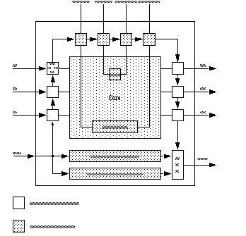
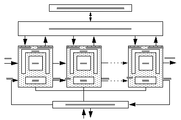
FIGURE 19. P1500 Architecture
P1500 supports set of mandatory and optional instruction listed in next chapters.
4.4.2 P1500 Optional Instruction
- WP/S_EXTEST - WBR is parallel / serial loaded for external test
- WP/S_PRELOAD - Data pre loaded into WBR via WSI / WSO with core in functional mode
- WS_CLAMP - Passes WP/S_PRELOAD data to the outputs of WBR cells. WBY selected and core is in test mode.
- WS_SAFE - Same as WS_CLAMP, but with hard wired values.
- WS_INTEST_RING - WBR used for core test
- WS_INTEST_SCAN - WBR used in serial with internal scan chain for core test.
5.0 Automated Test Pattern Generation (ATPG)
ATPG is process of generation of a test vector set for DUT that identifies defective devices on a tester. ATPG can be done by use of combinatial or sequential ATPG engines or combination of both.
Test vector set is sequence of input stimuli and output response for every tested I/O of the DUT. Each of the test vectors from the sequence is applied by the tester periodically at a time specified in the vector file.
Test vectors consist of test patterns (or parallel vectors) which represent parallel form of test vectors without scan-in and scan-out operation.
ATPG (for single fault model such as stuck-at-fault, bridging, delay/transition path models) is done by an ATPG tool and contains following tasks:
- Creating a fault list
- Collapsing equivalent (redundant) faults (Two faults are equivalent if there is no test that can distinguish between them)
- Removing asynchronous loops
- Marking destructive flip-flops
- Activating a fault to opposite state
- Propagating the fault effect to an output
- Marking covered faults in fault list
5.1 Combinatial ATPG
Combinatial ATPG is vector generation with a simplified view of the circuit. The combinatial ATPG engine sees the DUT as a purely combinatial circuit. Sequential elements represents virtual input and output ports (when they are part of scan chain) or black boxes (flip-flops which are excluded from scan chain) or pass through cells (in case of transparent latches). This type of engine is optimal for Full Scan or Almost Full Scan circuits.
- much faster then sequential ATPG engine
- better vector compaction
- can be used for very large chips (typically ATPG tools can handle designs of size about 8-10 Mgates)
Types of designs from test point of view:
5.1.1 Combinatial ATPG Rules (summary)
- No sequential elements are allowed. They are either made scannable (in scan chain) or black boxed (their output is modeled to hold ‘X’ value)
- All clocks of scannable sequential cells are controllable from primary inputs
- All presets of scannable sequential cells are controllable or disabled
- Non scan latches are made transparent or black boxed
- No memory primitives are allowed (black boxed or pass-through mode)
- No bus holders are allowed (if the ATPG tool cannot recognize them automatically, they have to be black boxed)
- No asynchronous logic allowed
- No asynchronous feedback loops allowed
- No clock signals fed to combinational logic.
Use of black boxed cells should be limited to minimum as they are decreasing testability of the DUT.
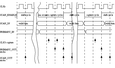
5.1.2 Combinatial Tester flow
- Input test vector is serially scanned in (shifted in) via scan input ports (shift cycle)
- Primary inputs are applied to the chip
- Optional pulse memories’ write enable (if memory is in pass-thorough mode)
- Strobe the chip’s primary output ports
- Apply system capture clock (capture cycle). Capture cycle might be applied in all clock domains together or in one clock domain only at same time (one hot clock decoding).
- Output response is serially scanned out (shifted out) via scan output ports
Steps 1 and 6 will overlap and occur simultaneously, except during the first and the last test cycle of the test.
5.2 Sequential ATPG
Sequential ATPG is test vector generation where faults can propagate across all storage elements (memories, bus repeaters, non scan latches, non scan flip-flops or scan flip-flops). Sequential ATPG engine is more sophisticated than combinatial, therefore it is slower (about 10 times) and cannot handle same design sizes (memory and performance limitation). This engine is applicable to any circuit (i.e. Full Scan, Almost Full Scan, Partial Scan,...)

7.0 Vector Verification
Vector verification in logic simulator is needed to verify, that the test vectors will work on a tester. A sample of test vectors (ideally full test vector set) should be verified with serial load. Full pattern set should be verified with parallel load (faster simulation due to much lower number of simulator events).
Vector verification is good at detecting various test protocol and timing issues (cross clock domain timing such as races).
8.0 Fault Simulation
Fault Simulation is process of evaluating the effectiveness of a test and to verify test coverage value reported by the ATPG tool. The test effectiveness is the test’s ability to detect faults and it is in direct relation with an acurancy of a fault model.
Fault simulators use following algorithms:
- Serial - slow (number of faults in the DUT times the functional simulation time), can detect all types of faults e.g. stuck-at, bridging, delay, even analogue faults. Speed can be improved by fault dropping.
- Parallel - only for circuits with logic gates, only for stuck-at faults, only in zero or unit delay, much faster than the serial fault simulators.
- Deductive - only for circuits with logic gates, only for stuck-at faults, only in zero or unit delay, faster than the parallel fault simulators as only the fault free circuit is simulated (faulty values are deduced from the fault free values).
- Concurrent - can detect various types of faults e.g. stuck-at, bridging and delay faults. Extends the event driven simulator model to handle simulation values as well as faults. Almost as fast as deductive fault simulators.
9.0 Vector Formatting
Generated test vectors have to be formatted for target simulator or tester. It is necessary to consider vector file size (vector file splitting). The size of vector files is dependent on length of scan chain. Mostly used test vector formats for testers are STIL and WGL. Use serial and parallel Verilog vectors for simulator.
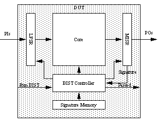
10.0 Built In Self Test (BIST)
BIST is like any other production test methodology mentioned before. It can support functional as well as structural test. The only difference is that the tester is not external to the IC, but it is built in the IC.
BIST aims to improve production test by following:
- Need less I/Os for testing
- At speed test (improved ability to detect faults)
- Improved diagnostic in field on board (if accessible via IEEE 1149.1)
- Can provide at speed burn in vectors
- Core reuse - embedded test (no need for additional test development
- Could be used for analog test (e.g. loop back)
- Trades test cost for chip area cost
- Possible self repair in RAM, FLASH type of application
- Can have timing impact.
- Can add to the design cycle.
BIST circuitry contain following parts:
- Input stimuli generator (ROM, FSM or Pseudo Random Pattern Generator (PRPG))
- Output response sampler
- Expected output response comparator with knowledge of expected response (ROM, signature)
- Pass / fail signal generator
- Self test controller
10.1 Logic BIST
Logic BIST typically uses pseudo random pattern input stimuli generated typically using Linear Feedback Shift Register (LFSR). The DUT has typically scan inserted. For circuits with multiple scan chains multiple output LFSR stimuli generator is used. The response is typically fed into a pattern compressor producing a signature. This signature is then compared to its stored “expected” value. The type of compression typically losses information. Therefore it is possible for a faulty DUT to produce correct signature (aliasing). Probability of the aliasing increases with the length of the test. In order to minimize the aliasing, the circuit response compression is typically done by multiple CRC modules using LFSR, by Multiple Input Signature Register (MISR). See principle diagram in Figure 22.
Problem of this structure is, that it often fails to test random pattern resistant faults on reasonable time. This can be solved by:
- Test point insertion.
- Weighted pseudo random pattern generator. Weight assignment is usually based on circuit analysis or fault detection probabilities.
- Reseeding LFSR.
10.2 Memory BIST (MBIST)
Memory BIST (MBIST) is widely used technique to test internal memories. This is because of the speed of BIST and the ease of generating test pattern for simple regular structure blocks such as memories. MBIST can be used for DRAMs, SRAMs, ROMs, Flash memories and register arrays. Multiple memories on chip can be tested by multiple or shared MBIST controller. Some MBIST controllers support diagnostic data output for failure analysis such as bit mapping.
Typical MBIST detects following faults in memories:
- Single cell stuck-at 0/1
- Single cell transition failure 0->1 / 1->0
- Single cell select open
- Multiple cell transition coupling (inversion - inverts content, idempotent - forces content to a fixed value, state - forces content to new state)
- Address decoder faults (no cell access, never accessed, multiple cell access, multiple address cell)
- Read/write stuck-at faults
- Timing faults (access, cycle, write recovery and data retention times)
Typical MBIST architecture is in Figure 23.
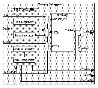
FIGURE 23. MBIST Architecture Principle
RAM memories are usually tested by March C-, MATS++, March LR and a retention test using a pause-polling mechanisms. Please see Philips 6N MATS++ algorithm or March C- 10N (Marinescu) algorithm. Due to its well known theoretical background, acceptable test time (10N) and good fault coverage (96-99.99% for single fault) March C- is the most popular MBIST algorithm. The March C- 10Nalgorith is a follows:
- write 0 in either ascending or descending order
- read 0 and write 1 in ascending order
- read 1 and write 0 in ascending order
- read 0 and write 1 in descending order
- read 1 and write 0 in descending order
- read 0 in either ascending or descending order
MATS++ 6N algorithm is as follows:
- write 0 in either ascending or descending order
- read 0 and write 1 in ascending order
- read 1, write 0 and read 0 in descending order
Following table compares MATS++ and March C- tests.
Where: SAF - Stuck-at Faults, AF - Address Fault, CFin - Coupling Fault - inversion, TF - transition faults, CFid - Coupling Faults - idempotent, CFdyn - Coupling Faults - dynamic, SCF - State Coupling Faults.
ROM memories are typically tested by 2N (read followed by inverse read) read algorithm with CRC (MISR) compactor and signature comparator. For better resistance to signature aliasing, the resulting signature can be calculated from the memory content itself as well as from its complement.
11.0 Boundary Scan Test (IEEE 1149.1)
The reason for boundary scan, is to test for board assembly and manufacturing defects listed below:
Boundary scan can be used to test:
- board interconnect (Extest) - tests for opens, shorts, correct part alignment, correct packaging
- functionality of the core of an IC (Intest) - limited functionality tests such as part existence, correct part ID, internal BIST control, parametric test of I/Os
The testing outlined above is done through boundary scan cells at the edge of an IC in between its pads and the chip core. These boundary scan cells allow to observe logic values from either primary inputs (PI) or outputs from the core. These boundary scan cells can also control the values passed to the chip core or to chips primary outputs (PO). Additionally all the boundary scan cells are internally connected into a scan chain called boundary scan register (BSR).
Boundary scan functionality is controlled by Test Access Port (TAP) Controller via its state machine and set of instruction passed to Instruction register.
Access to all the registers within the boundary scan test structures is provided by means of shifting the desired data in from TDI.
One bit bypass register provide rapid access from TDI to TDO.
Optional 32 bit identification (ID) number register capable of being loaded with permanent ID code provide means of unique identification of each particular IC.
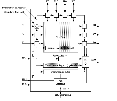
Architecture of IEEE 1149.1 chip is outlined in Figure 24.
In order to allow testing of multiple devices, all shift in data are shifted through to TDO output which can be connected to TDI of a next IC on the board. See Figure 27.
11.1 Architecture
The IEEE 1149.1 architecture consists of following parts:
- Boundary Scan Register (BSR) formed as a chain of boundary scan cells for each primary input, output and bidirectional port.
- Test Access Port (TAP) - four wire interface (TDI, TMS, TDO, TCK) plus optional TRST pin
- Instruction Register (IR) holding current instruction
- Test Access Port Controller controlling the function and sequencing of events in boundary scan
- 1 bit bypass register
- Optional 32 bit identification register loadable with permanent device ID number
For details see Figure 24.
11.1.1 Test Access Ports
- TDI - test data input - serial data in, sampled on rising edge. Default = 1.
- TDO - test data output - serial data out, changes on falling edge. Default = Z.
- TMS - test mode select - input control, sampled on rising edge. Default = 1.
- TCK - test clock - any frequency (typically 10 MHz)
- TRST - test asynchronous reset (optional) - active low. Default = 1. There is always synchronous reset mechanism implemented in TAP Controller (TMS = 1 for 5 TCK cycles).
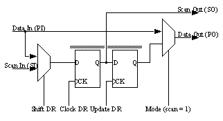
11.1.2 Boundary Scan Cell
Figure 25 shows a concept of basic boundary scan cell known as BC_1. The cell can operate in four modes:
- Normal - Data_In is passed to Data_Out
- Update - content of Update Hold Cell is passed to Data_Out
- Capture - Data_In is captured to Capture Scan Cell by next Clock_DR (derivative of TCK)
- Serial shift - Scan_In is captured by Capture Scan Cell while Scan_Out output is connected to Scan_in of the next cell in Boundary Scan Register (BSR).
Both Capture and Shift operations do not interfere with Normal mode of operation. This allows capture of Data_In values while the device is in normal (functional) mode of operation.
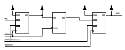
11.1.3 Instruction Register
Instruction register has scan shift section connected between TDI and TDO, hold section holding current instruction and possibly also some decoding logic used to generate control signals selecting TDI/TDO access to each individual register within boundary scan. See Figure 26 for Instruction Register principle.
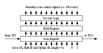
FIGURE 26. Instruction Register
Instruction Register must support four mandatory instruction:
- Extest - Used to test board interconnects. BSR is selected and the device is in test mode. PI BS cells have permission to set core inputs and PO BS cells have permission to set POs.
- Bypass - Used for quick access to another device on the board. Bypass register is selected.
- Sample - Used to capture functional mode signals into BS cells. BSR selected and device is in functional mode.
- Preload - Used to preload BS cells with values. BSR selected and device is in functional mode.
Supporting those instructions mean that the minimum length of Instruction register is 2 bit, maximum length is not defined. Apart from these mandatory instructions IEEE 1149.1 define six optional instructions:
- Intest - Used to test the device’s core. BSR selected and BS cells have permission to set their outputs.
- Idcode - Used to capture devices 32 bit ID. Optional ID register selected.
- Usercode - Used to capture an alternative user ID (e.g. in programmable devices). Optional ID register selected.
- Runbist - Used to run internal BIST in the device and output its status (pass/fail). Pass fail register is selected together with a register for initiating the internal BIST sequence. Chip is in test mode with safe PO values set using Preload instruction.
- Clamp - Uses to set devices PO to safe mode (e.g. to avoid bus contention). Bypass register is selected with known PO values set using Preload instruction.
- HighZ - Used to put devices POs to high impedance state. Bypass register is selected. Values to drive POs to their high impedance state are pre-loaded using Preload instruction.
IEEE 1149.1 allows usage of any number of private instructions providing access to other internal registers. For example an instruction which allow access to scan chain(s).
Please note, that all unused Instruction codes must default to Bypass.
11.1.4 TAP Controller
Tap Controller is 16 state Moore FSM. Inputs are TMS, TCK and optional TRST. It generates following control signals for Instruction Register (Clock_IR, Shift_IR and Update_IR) and signals for other data registers (Clock_DR, Shift_DR and Update_DR)
Design of TAP Controller guarantees that for any register selected between TDI and TDO, there are always three operations performed on the register in following fixed order:
11.1.5 Boundary Scan Description Language (BSDL)
BSDL (Boundary-Scan Description Language) files are necessary for the application of boundary-scan for board and system level testing and in-system programming. BSDL files describe the IEEE 1149.1 design within an IC, and are provided as a part of their device specification.
11.1.5.2 BSDL example
entity XYZ is
generic (PHYSICAL_PIN_MAP : string := "DW");
port (OE:in bit;
Y:out bit_vector(1 to 3);
A:in bit_vector(1 to 3);
GND, VCC, NC:linkage bit;
TDO:out bit;
TMS, TDI, TCK:in bit);
use STD_1149_1_1994.all;
attribute PIN_MAP of XYZ : entity is PHYSICAL_PIN_MAP;
constant DW:PIN_MAP_STRING:=
"OE:1, Y:(2,3,4), A:(5,6,7), GND:8, VCC:9, "&
"TDO:10, TDI:11, TMS:12, TCK:13, NC:14";
attribute TAP_SCAN_IN of TDI : signal is TRUE;
attribute TAP_SCAN_OUT of TDO : signal is TRUE;
attribute TAP_SCAN_MODE of TMS : signal is TRUE;
attribute TAP_SCAN_CLOCK of TCK : signal is (50.0e6, BOTH);
attribute INSTRUCTION_LENGTH of XYZ : entity is 2;
attribute INSTRUCTION_OPCODE of XYZ : entity is
"BYPASS (11), "&
"EXTEST (00), "&
"SAMPLE (10) ";
attribute INSTRUCTION_CAPTURE of XYZ : entity is "01";
attribute REGISTER_ACCESS of XYZ : entity is
"BOUNDARY (EXTEST, SAMPLE), "&
"BYPASS (BYPASS) ";
attribute BOUNDARY_LENGTH of XYZ : entity is 7;
attribute BOUNDARY_REGISTER of XYZ : entity is
"0 (BC_1, Y(1), output3, X, 6, 0, Z), "&
"1 (BC_1, Y(2), output3, X, 6, 0, Z), "&
"2 (BC_1, Y(3), output3, X, 6, 0, Z), "&
"3 (BC_1, A(1), input, X), "&
"4 (BC_1, A(2), input, X), "&
"5 (BC_1, A(3), input, X), "&
"6 (BC_1, OE, input, X), "&
"6 (BC_1, *, control, 0)";
12.0 IDDQ test
IDDQ test is based on measuring the leakage current of the DUT. It is based on the assumption, that the leakage current of good devices is different than the leakage current of the bad ones. See Figure 28 for IDDQ fault distribution example. IDDQ test cannot detect faults like open connection or connection to wrong sink, but it is suitable for detection of faults like:
- Low treshold voltage of transistors
- Low resistance of gate oxide
- Resistive bridges
- Punch trough
- Leaky junctions
- Parasitic leaks
- Shorts to rails
IDDQ test is performed by applying a test pattern followed by wait period to allow for transistors to “settle” followed by Vdd current measurement. If the correct current value is lower than the treshold, then the device is considered to be good, if the current is bigger, the device is faulty.
Current measurement can be performed on chip as well as off chip.
In order to be able to measure IDDQ current successfully, all not CMOS circuits drawing static current (analog blocks, PLLs, ring oscillators, DRAMs, pull up/down, etc.) has to be powered down.
Detecting faults in IDDQ test requires test patterns which create conductive path from Vdd to GND. The test patterns are basically stuck-at patterns which provide the propagation of the fault to the gate output, these are called “pseudo stuck-at patterns”.
With shrinking feature size, the leakage current of a circuit is growing dramatically (Ioff in 0.18um is about 10x of Ioff in 0.35um technology) while Ron of a transistor is increasing. This increase in IDDQ is masking the faults present in the circuit and leads to too many escapes or to binning good chip if the treshold is set too close to Mg (see Figure 28). Solution of the problem can be:
- Using current signatures for each test pattern
- Use of Delta IDDQ
- Substrate biasing in order to increase Vt
- Power supply partitioning of an IC
- Adaptive IDDQ treshold based on neighbor chip matching on a die
- Use of IDDT
There is little evidence that Low Voltage Tests (LVT) actually add additional test coverage on the top if IDDQ (IDDT) test.
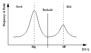
FIGURE 28. IDDQ: Fault Distribution Curve - Example
Even though IDDQ (IDDT) tests are good at detecting many different types of defects, it cannot help to locate them.
12.1 Delta IDDQ
The goal of this methods is to reduce the variance in fault-free IDDQ in order to make distinction between fault-free and faulty leakage. Delta IDDQ relies on the assumption that variation in fault-free IDDQ is expected to be small so if differences are taken between two vectors the Differences are close to zero. The variations in IDDQ caused by the process variations and vector sensitivities are random by nature and therefore should cancel out, so mean Delta IDDQ should be close to zero.
12.2 IDDT
On the contrary to the IDDQ leakage current (static) test IDDT test is base on measuring the transient supply current of the DUT. IDDT observes the peak value of IDDT as well as the shape and the duration of the peak during switching of a circuit state. The transient current can be measured, for example, by integrating the IDDQ over specific time interval. Manufacturing defects, when activated, will cause higher or lower measured IDDT value.
13.0 Near Future Outlook
In the immediate future DFT will most likely be dominated by scan test using stuck-at, delay and bridging fault models with more emphasis on at speed testing. At speed testing will be more used as stuck-at test are more effective when run at speed. There will probably be significant increase in the use of various logic BIST solutions. Logic BIST will be more used in IP block testing.
In order to be able to deliver ever increasing amount of test patterns into DUT pattern compression / decompression interfaces will be used.
Delay fault tests will also be used more as interconnect and its parameters are starting to be dominant in DSM.
P1500 structured test is likely to be more widespread either due to their scalability (chip size) or due to block and test reuse.
IDDQ will be most likely replaced by a dynamic test such as IDDT in technologies with feature sizes below 90/65 nm.
Ring oscillators will be used more because of its potential of simply detecting the “speed of silicon”.
15.0 Appendix
15.1 Design Examples
15.1.1 Device 1
- Dual Technology - 2.5V core logic and 3.3 I/O cells etc.
- 950kgates
- Memory with BIST - untestable by scan
- Boundary scan
- Macros - untestable by scan
- 12 clock domains
- Hierarchical gate level netlist
- Fault Coverage 95.38%
- Fault Efficiency 100%
- Vector Count 7521 parallel vectors (58.3Mvectors) (TPG2)
- Test vector frequency 25MHz ==> 2.33sec test time
- 4 scan chains 7749 length each
-
Run time (1998):
compilation - 4 -5 hours
scan insertion - about. 20 hours
DRC - about. 15 hours
ATPG - 2 -3 days
vector compaction about. 2 days
vector formatting - 1 day
vector verification - 5 parallel vectors about 8 hours
IKOS verification - about. 2 months run time for FUNC, MIN and MAX cases - test vector file splitting - 76 vector files - 100 parallel vectors each
- IDDQ Test: 10 parallel vectors IDDQ coverage 63%
15.1.3 Device 3
- 50 kgates
- 5 clk domains
- 2 power domains
- 2 scan chains
- scan chain length: 1610
- 85 scan excluded Dffs
- ~ 200 not fixed DRC violations
- many not controllable clocks, presets
- many feedback loops
- design not strictly synchronous (clocks as input to logic)
- Test coverage: 90.46% (stuck at)
- Pattern count: 638
- Test time: 30,921,780.00 NS
- IDDQ patterns: Test coverage: ~ 70% (73.21% stuck at), pattern count: 12